


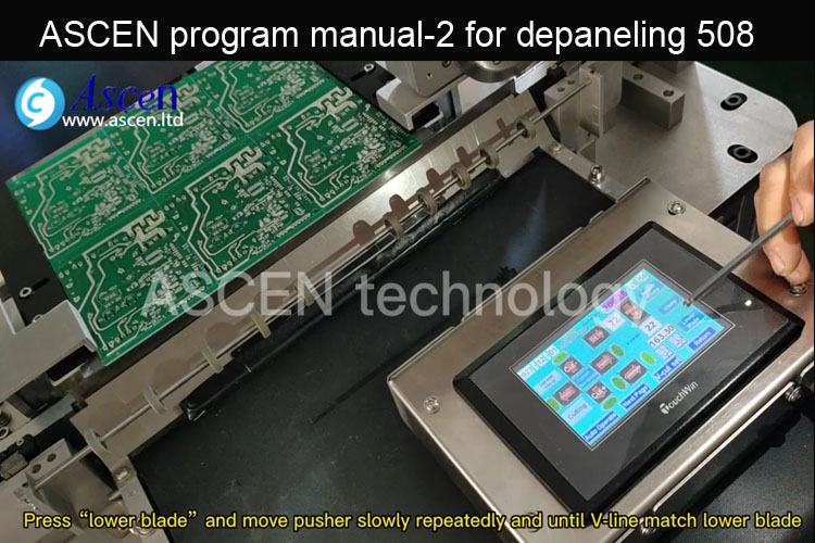
This is the part 1 of high speed PCB depaneling router programming manual,you can detailed understanding ASCEN PCB router machine function and the operation interface via ASCEN video manual,learn how to program and drawing routing track diagram,help you process troubleshooting and solve machine fault.
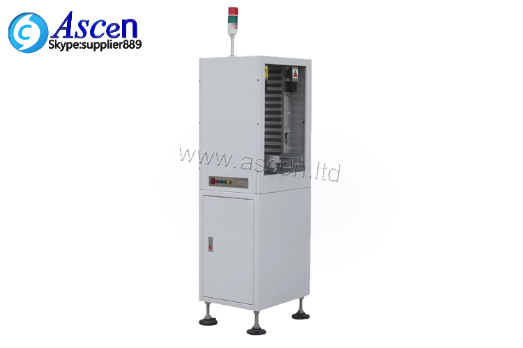
High speed PCB depaneling router is used to depanel PCB’s using a programmable router.The PCB depaneling router takes a multiple module printed circuit board and cuts out (depanels) individual printed circuit boards leaving a scrap frame.desktop version PCB milling router with a high cost performance and very popular in the small and medium manufacturers,ASCEN PCB router depaneling machine can offline mode operation and also can as a online PCB routing depaneler to connect your robot arm for automatic pick up the PCB board.to arrival the high automation production.
By the way,if your company need more efficient PCB depaneling router machine,you can click video link here double station PCB router machine to check the large scale PCB router depaneling machine how to quickly connect the robot.
By the way,if your company need more efficient PCB depaneling router machine,you can click video link here double station PCB router machine to check the large scale PCB router depaneling machine how to quickly connect the robot.
ASCEN PCB router depaneling machine AS-3A/4A model,the programming manual total 1-9 part.please check the following link to see the detail:
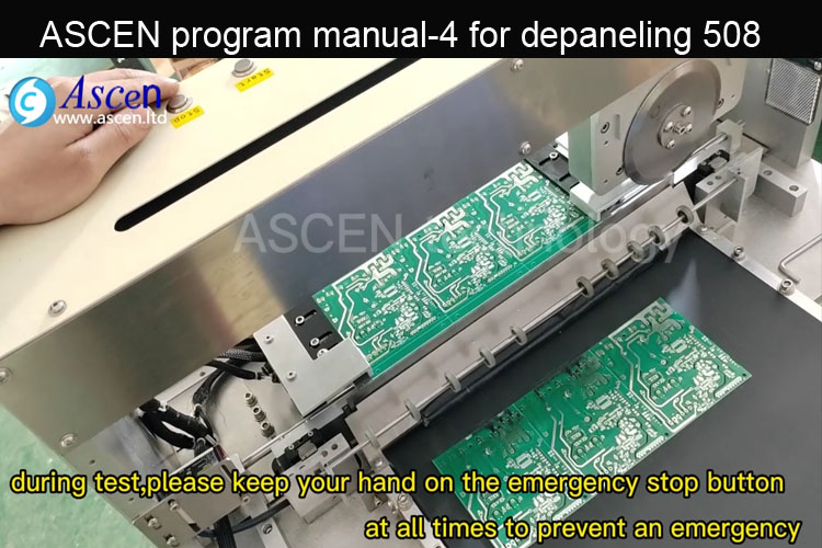
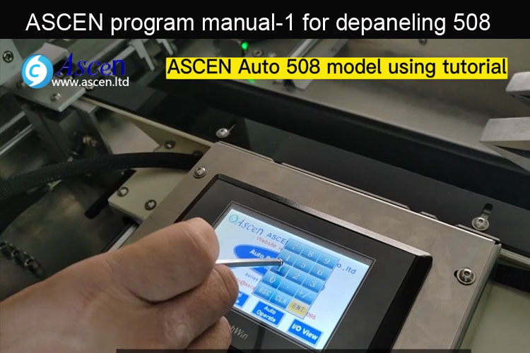
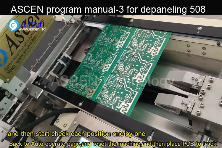
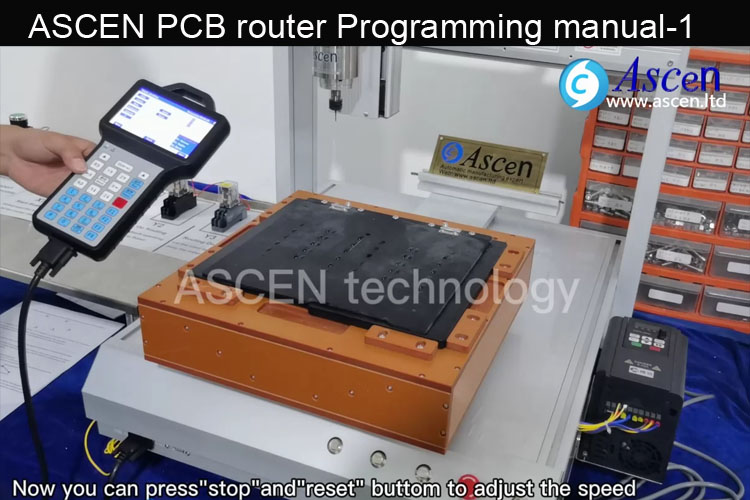
PCB depaneling router manual part 1, learn PCB router machine function and the operation interface
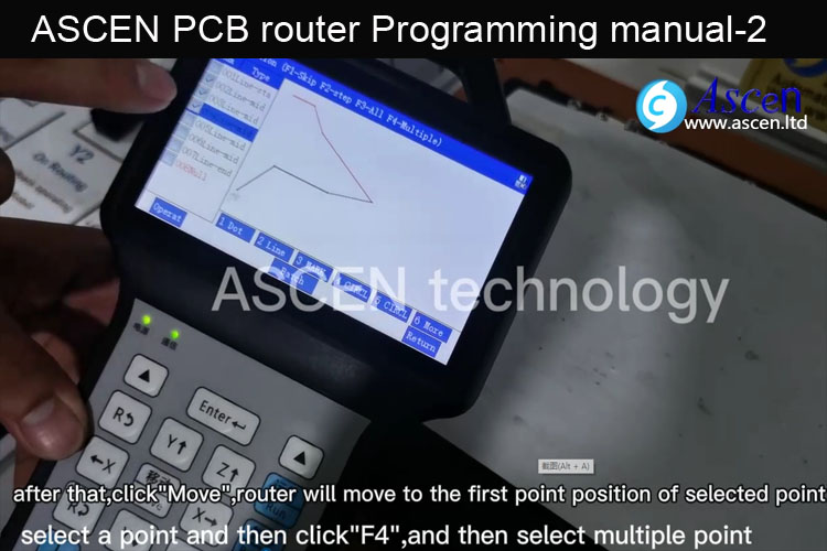
PCB depaneling router manual part 2, learn PCB router machine "Move and edit"function
PCB depaneling router manual part 3, learn PCB router machine "Insert instruction"
PCB depaneling router manual part 4, learn PCB router machine "copy instruction"
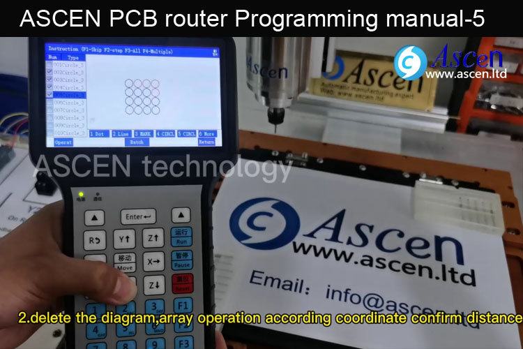
PCB depaneling router manual part 5, learn PCB router machine "Array replication"function and offset operation
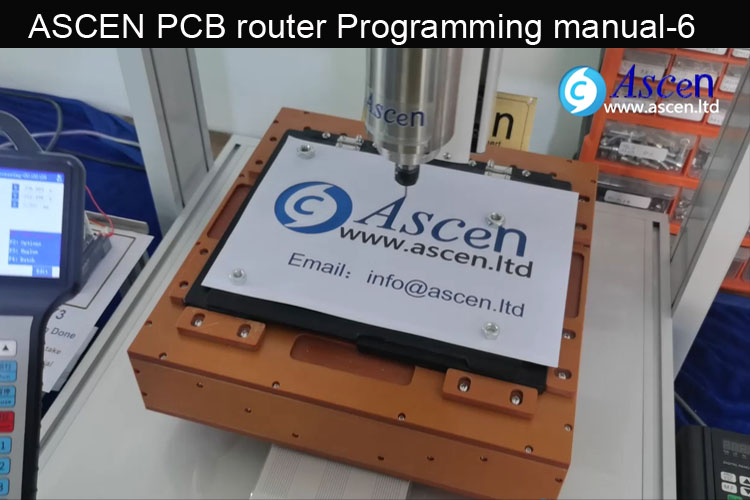
PCB depaneling router manual part 6, learn PCB router machine modify parameters
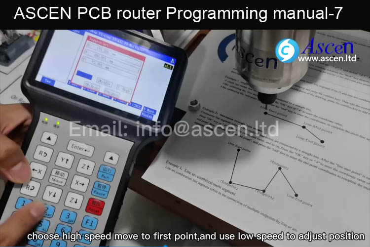
PCB depaneling router manual part 7, learn PCB router machine "Dot" and "Line"instruction
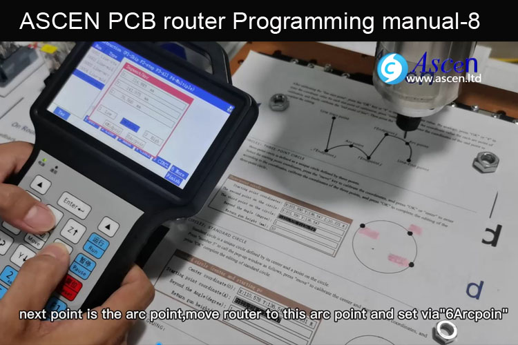
PCB depaneling router manual part 8, learn PCB router machine “Line arc combined multi segment” instruction
PCB depaneling router manual part 9, learn PCB router machine drawing diagram via PCB panel